41 p type semiconductor band diagram
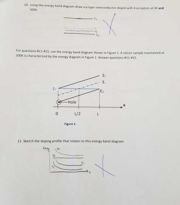
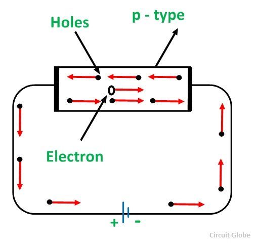
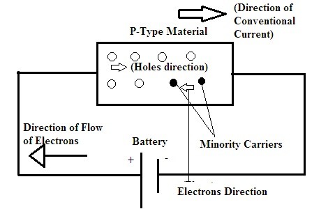
The energy band diagram of a p-Type Semiconductor is shown below. A large number of holes or vacant space in the covalent bond is created in the The electrons available in the conduction band of the n type semiconductor are much more movable than holes available in the valence band in a p... We all know that in semiconductor crystal each tetra valiant atom creates covalent bond with four neighboring atoms. In this way, each of the Finally, we can say that in a p-type semiconductor has plenty of holes move randomly inside the crystal. In addition to holes generated due to trivalent...
In these E-k diagrams, often called band diagrams, plotted in what is referred to as a reduced zone scheme, the momentum that is plotted is actually a Doped semiconductors (either n-type or p-type) are known as extrinsic semiconductors. The activation energy for electrons to be donated by or...

P type semiconductor band diagram
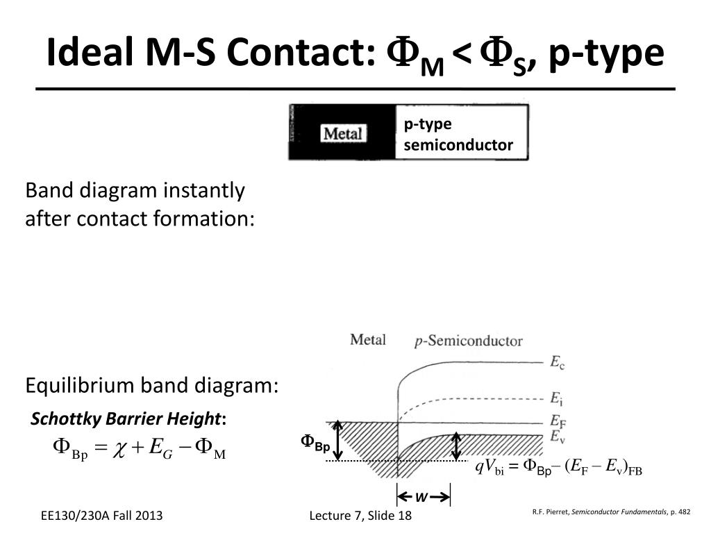
Energy-band diagram/animation for a p-type, reverse biased metal-semiconductor schottky contact. For more information on metal-semiconductor ohmic and... An n-type semiconductor is created when pure semiconductors, like Si and Ge, are doped with pentavalent elements. As can be seen in the image above, when a pentavalent atom takes the place of a Si atom, four of its electrons The above energy band diagram is of p-type Si semiconductor. Modern Semiconductor Devices for Integrated Circuits (C. Hu). Slide 1-6. 1.3.1 Energy Band Diagram. Conduction band Band gap. Eg. If light shines on the N-type semiconductor and generates area A holes (and electrons) at the Jp(x) Jp(x + ∆x) rate of G s-1cm-3
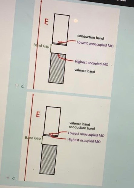
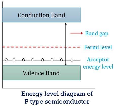
P type semiconductor band diagram. Energy Band Diagram of p-Type Semiconductor. The energy band diagram of a p-type Semiconductor is shown below: A large number of holes or vacant space in the covalent bond is created in the crystal with the addition of the trivalent impurity. File:P-Type Semiconductor Bands.svg. From Wikimedia Commons, the free media repository. Jump to navigation Jump to search. Diagram of the conduction and valence bands in a p-type semiconductor above 0K. Date. 9 hours ago Band Diagram • We will start by drawing the band diagram in equilibrium (flat band condition). Metal Insulator P-Type Semiconductor • We will today consider p-type semiconductors, but as usual, the theory is general. ... A p-type semiconductor is an extrinsic type of semiconductor. When a trivalent impurity (like Boron, Aluminum etc.) is added to an intrinsic or pure semiconductor (silicon or germanium), it is said to be a p-type semiconductor.
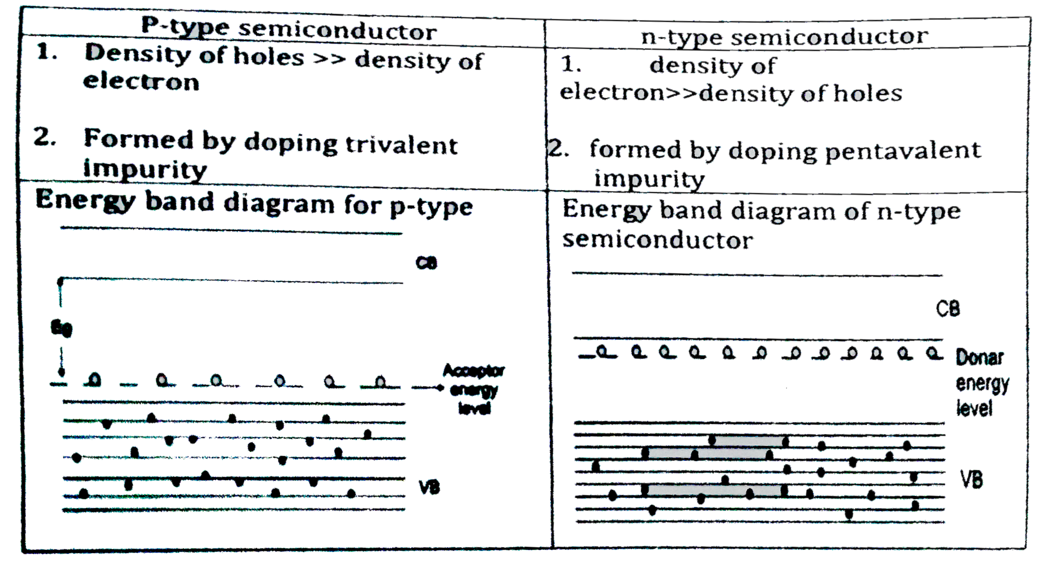
Difference between P-type Semiconductor and N-type Semiconductor. We know that the p-type and n-type semiconductors come under extrinsic What is P-type Semiconductor and N-type Semiconductor? The definitions of p-type and n-type and their differences are discussed below. Diagram of the conduction and valence bands in a p-type semiconductor above 0K. File:P-Type Semiconductor Bands.svg. From Wikipedia, the free encyclopedia. Even though p-type semiconductor has large number of holes, but these holes is provided by the trivalent atoms that are electrically neutral. In p-type semiconductor, the population of holes in valence band is more, whereas the population of free electrons in conduction band is less. In solid-state physics of semiconductors, a band diagram is a diagram plotting various key electron energy levels (Fermi level and nearby A band diagram does however try to show the changes in the band structure from place to place. In doing so, there is an intrinsic conflict due to the Heisenberg...
• The band diagram of a semiconductor-vacuum interface is shown. • Near the surface, the n-type semiconductor is depleted of free electrons due to the pinning of the Fermi level near the middle of the forbidden gap at the semiconductor surface. Semiconductors are materials that possess the unique ability to control the flow of their charge carriers, making them valuable in applications like cell phones, computers, and TVs. An extrinsic … Besides the E(x) band diagram of Fig. 2.2, there is the more detailed energy band representation in k-space, E(k), which allows further insight into If in a p-type semiconductor the hole current is in principle achieved by a motion of valence electrons as in the classical bubble model, the Hall constant... Energy Diagram of P-Type Semiconductor. As it is doped with trivalent impurity there are a huge number of holes formed in the p-type. P-type because of majority a-holes it referred to as a positive type. As it is a p-type semiconductor the Fermi level is present near to the valence band rather than...
• Band Diagram - in a band diagram, we tabulate the relative locations of important energy levels. • P-type Doping - this extra electron increases the p-type charge carriers - we call this type of charge - this can be seen in the band diagrams by "bending" the mid-gap (or Ei) energy at the surface of the...

For a lightly doped semiconductor the bands are flat, whereas the band curvature increases as the doping level increases. Variously doped n-type structures (dopant concentration between 1.5 * 10(16) cm(-3) and 1.5 * 10(19) cm(-3)) on a lightly doped p-type silicon substrate (doped to 1.9 * 10...
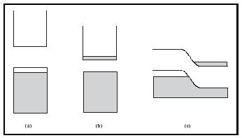
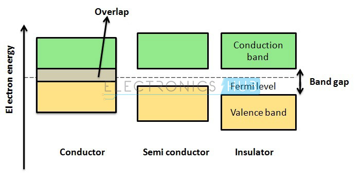
The band diagram of an insulator is similar to that of a semiconductor except for a larger Eg FIGURE 1-13 Energy band diagrams for a semiconductor (a), an insulator (b), and a conductor It can be doped N type and P type, and electronic devices such as rectifiers and transistors have been...
In solid-state physics of semiconductors, a band diagram is a diagram plotting various key electron energy levels (Fermi level and nearby energy band edges) as a function of some spatial dimension, which is often denoted x. These diagrams help to explain the operation of many kinds of...
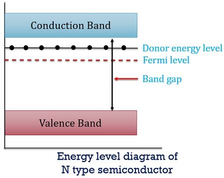
KEYWORDS Semiconductor · intrinsic conduction · extrinsic conduction · energy band gap · conduction band · valence band · conductivity An extrinsic semiconductor, in which conduction electrons are the majority carri-ers is an n-type semiconductor and its band diagram is illustrated in...
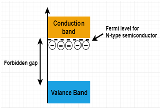
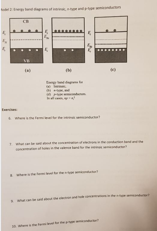
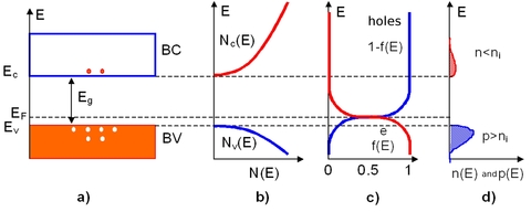
Electron energy band diagrams for semiconductors, metals, and insulators, (a) n-type semiconductor. (b) p-type semiconductor. Largely filled valence band lies below EV and largely empty conduction band-lies above EC. The Fermi level lies closer to EC in the n-type...

Bands in Intrinsic Semiconductors. The band structure of any real crystalline semiconductor is quite complicated and allows for different types of behavior. 4: Aggregate band diagram for an intrinsic semiconductor.
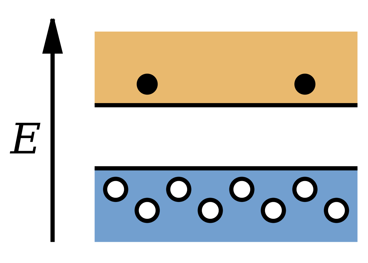
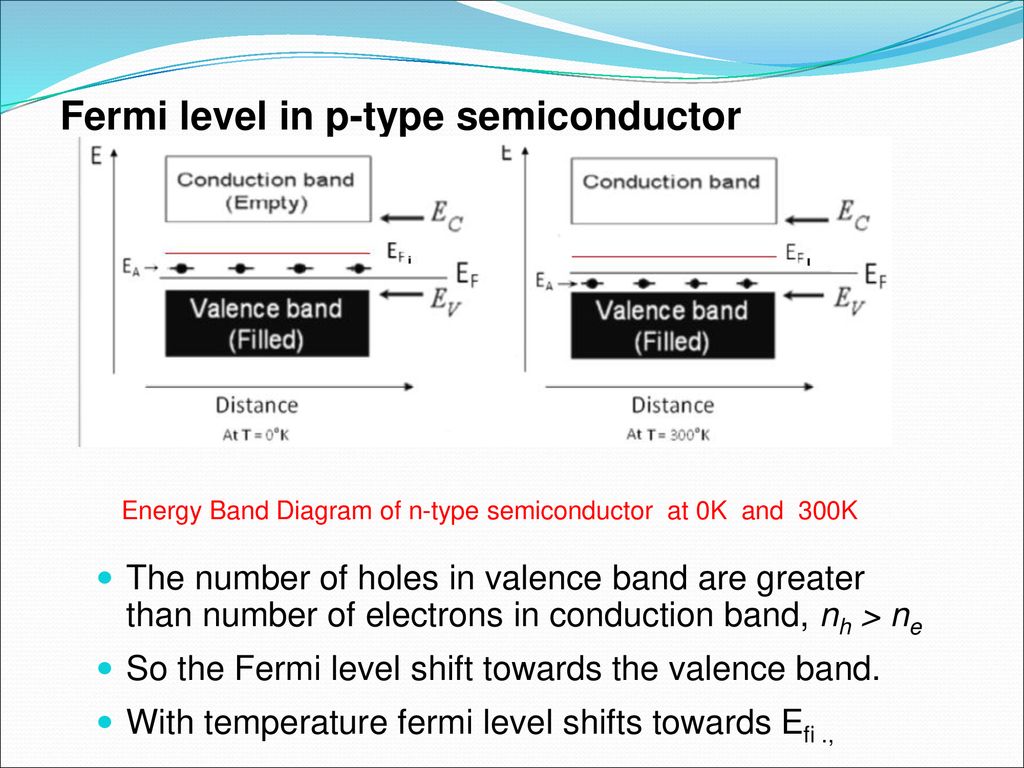
The above figure shows the energy band diagram of p-type semiconductors. For this type of semiconductors, the Fermi level shifts towards the valence band. Because, the density of positive holes becomes higher for p-type semiconductor than its intrinsic counterpart.
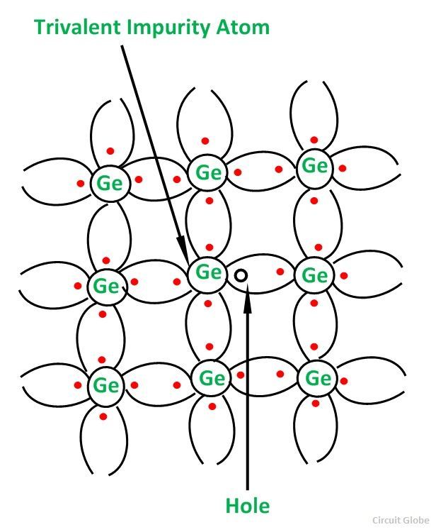
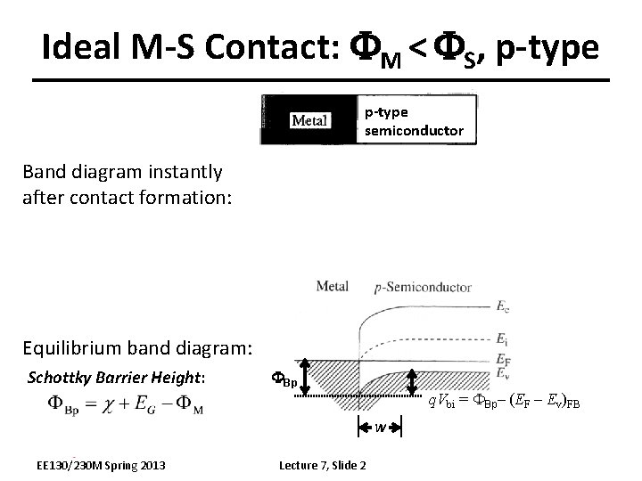
Figure 2: Energy band diagram of p and n type Si before the junction is formed. The location of the Fermi level is dierent for the two semiconduc-tors. 2 Contact potential. Consider a junction between p type and n type Si. The band diagrams of the two semiconductors, where apart, are shown in gure...

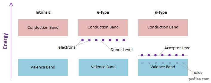
Band diagrams can help us understand conductors, semiconductors, and insulators. Using the band gap diagram, you can think of doping as adding possible energy states. N-type doping adds new levels for electrons below the conduction band, and P-type doping adds new energy levels above the...
The energy band diagrams at temperature of the n-type and p-type extrinsic semiconductor are shown in Fig. Draw the energy band diagrams for an n-type semiconductor to illustrate the difference between the two types. 2.11. Consider a p-type semiconductor doped with boron of...
Types of Semiconductors Semiconductors can be classified as: · Intrinsic Semiconductor · Extrinsic Semiconductor Intrinsic Semiconductor An intrinsic type of semiconductor material is made to be very pure chemically. Energy Band Diagram for Semiconductors, Conductors, and Insulators.

Modern Semiconductor Devices for Integrated Circuits (C. Hu). Slide 1-6. 1.3.1 Energy Band Diagram. Conduction band Band gap. Eg. If light shines on the N-type semiconductor and generates area A holes (and electrons) at the Jp(x) Jp(x + ∆x) rate of G s-1cm-3
An n-type semiconductor is created when pure semiconductors, like Si and Ge, are doped with pentavalent elements. As can be seen in the image above, when a pentavalent atom takes the place of a Si atom, four of its electrons The above energy band diagram is of p-type Si semiconductor.
Energy-band diagram/animation for a p-type, reverse biased metal-semiconductor schottky contact. For more information on metal-semiconductor ohmic and...


0 Response to "41 p type semiconductor band diagram"
Post a Comment